Decapped BMS Chips
|
I've been slowly accruing a collection of battery monitoring system (BMS) chips, each designed to monitor a stack of battery cells in a multi-cell battery pack. Other than the die area and what's in their publicly-available datasheets, I don't say much about them. I designed the secondary bandgap reference on the MAX17823. |

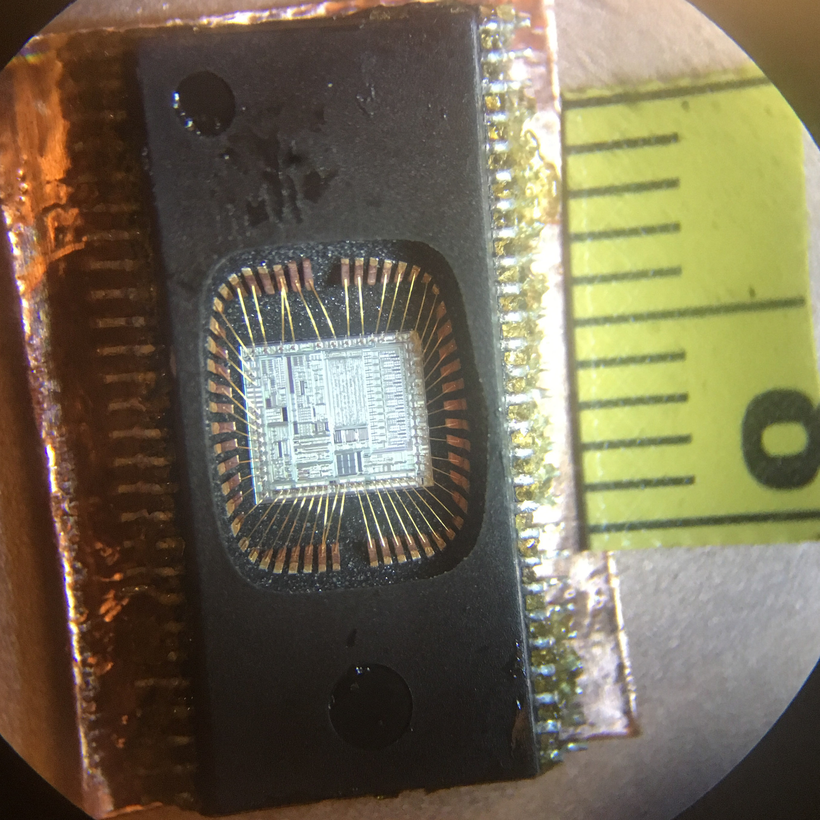
A yellow tape measure with black millimeter marks was used to estimate die size in the following photos. The estimates are probably within about 10%. Click on any photo for a higher resolution image.
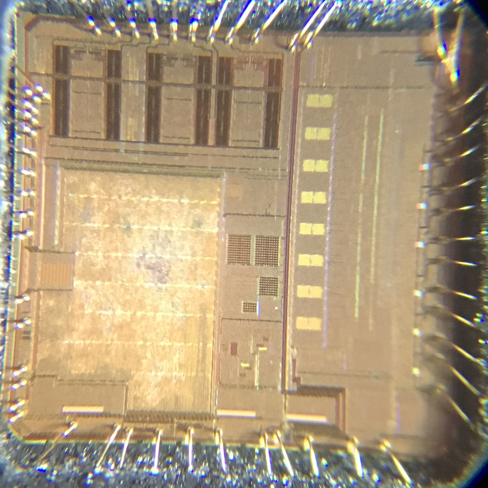
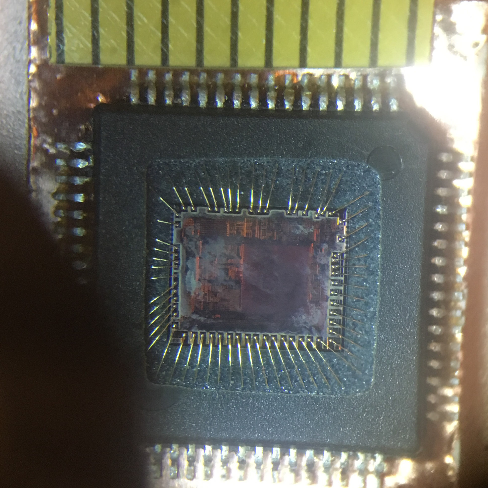
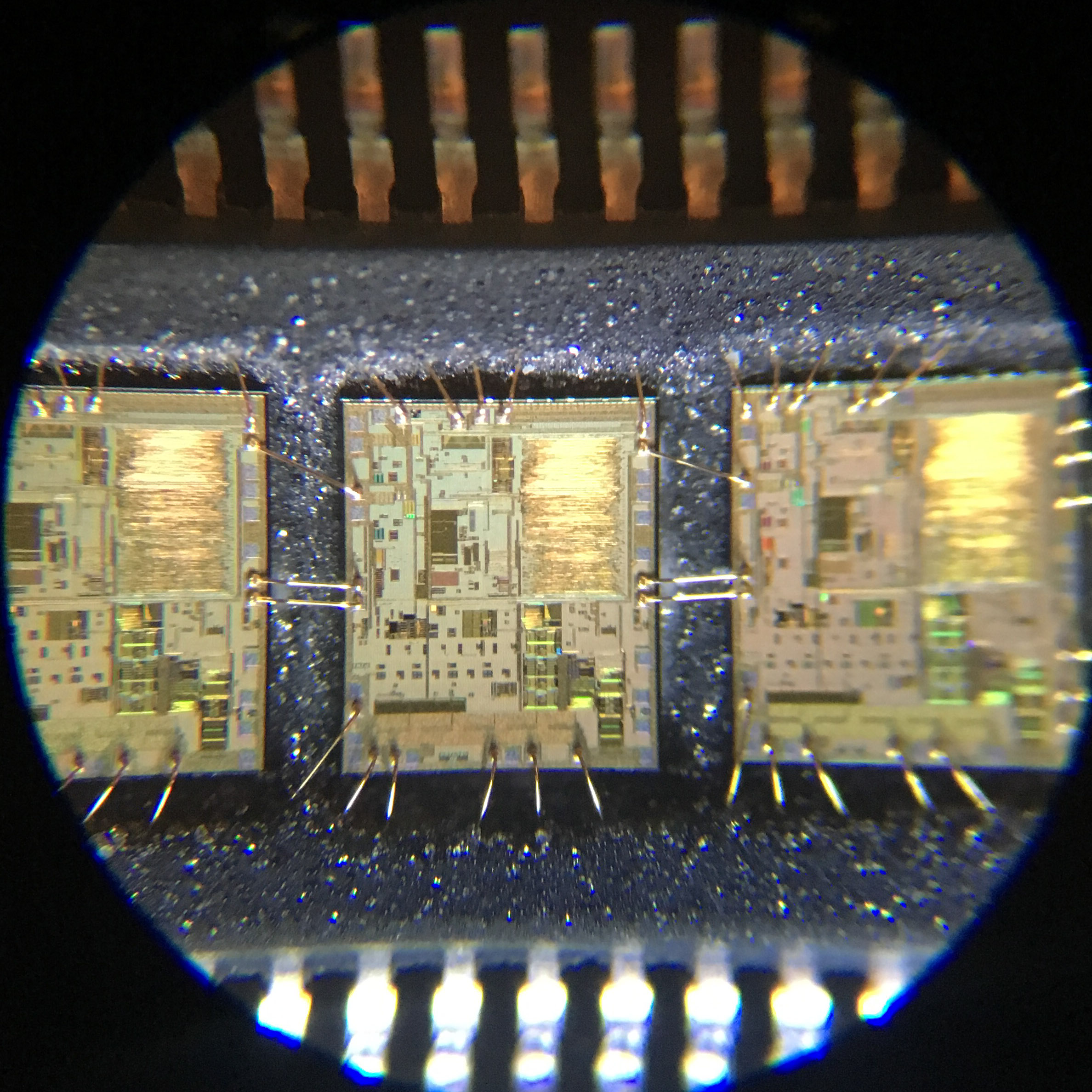
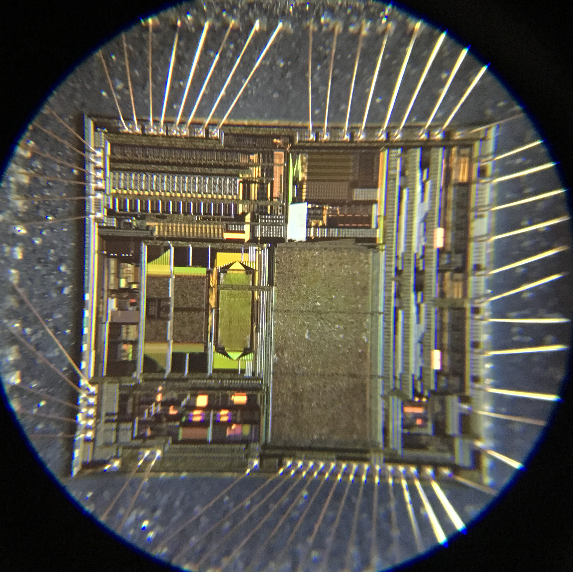
| ST L9963E | 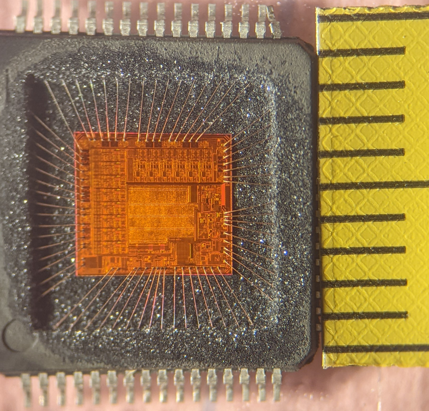
| 
| Die area: 4.34mm x 4.79mm = 20.8mm2 Channel count: 14 AEC-Q100 The orange color and what looks like a puddle... I sort of wonder whether this chip was coated in die coat, which relieves package stress and thus can improve accuracy, and whether the puddle is an artifact of the decapping chemicals interacting with the die coat. |
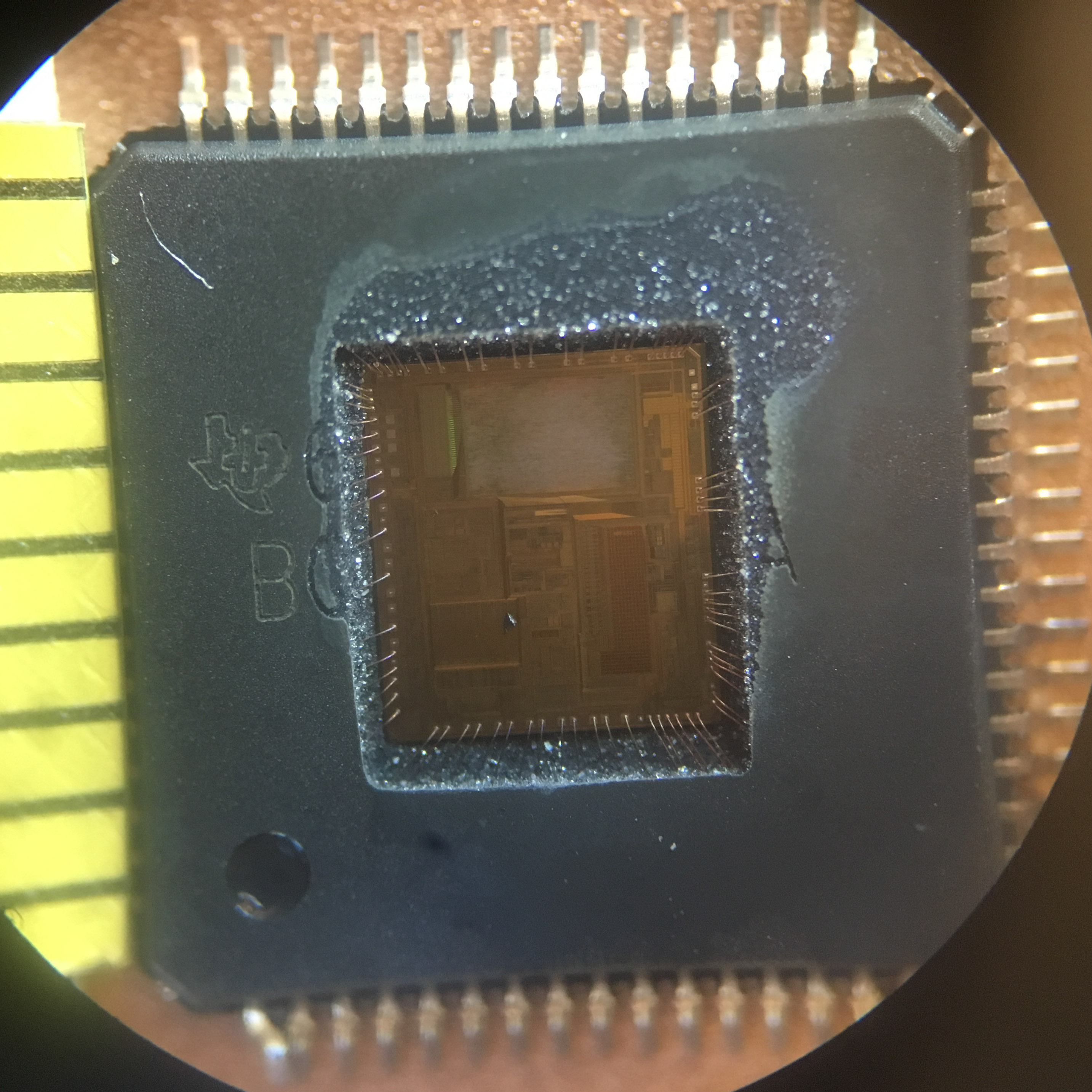
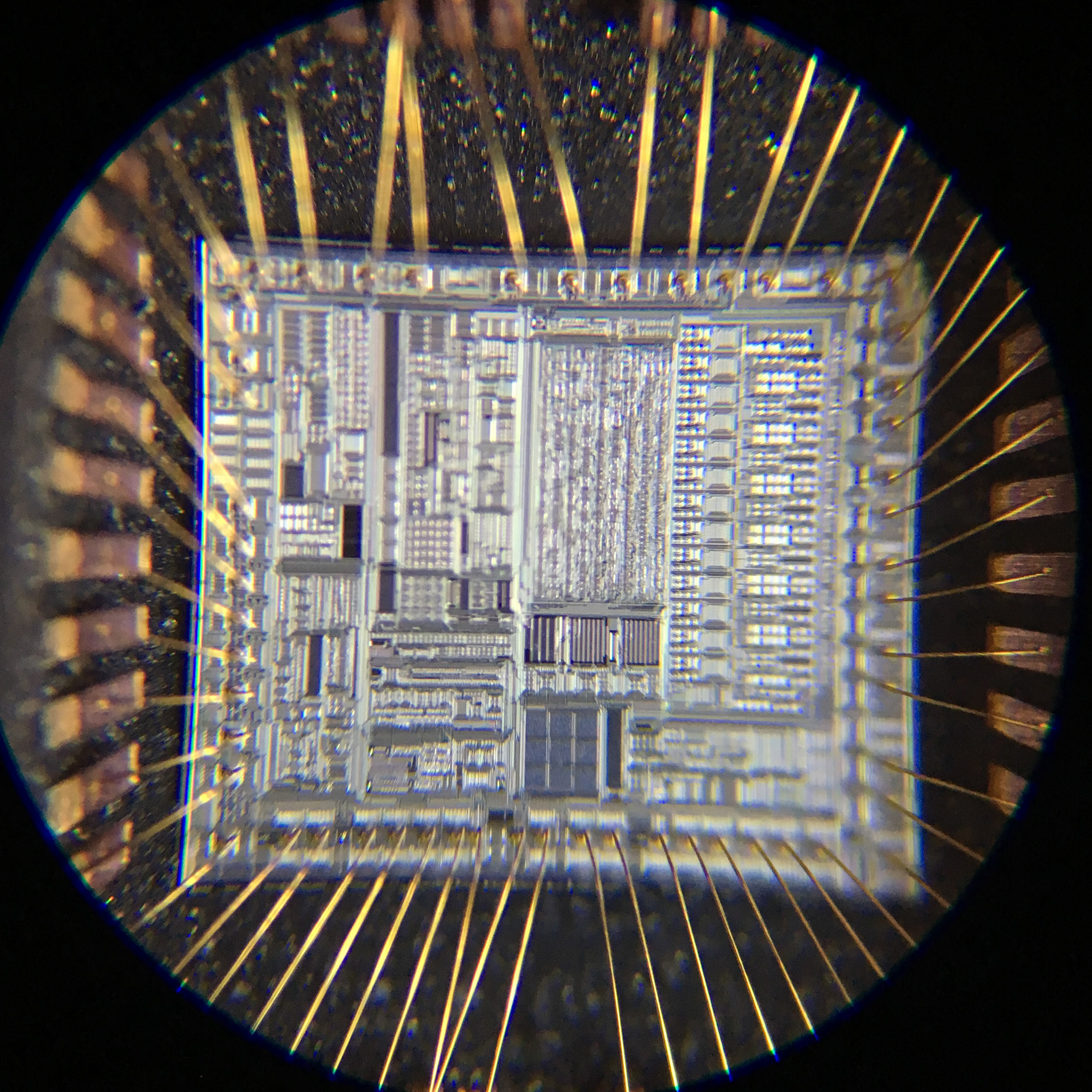
| NXP MC33771C | 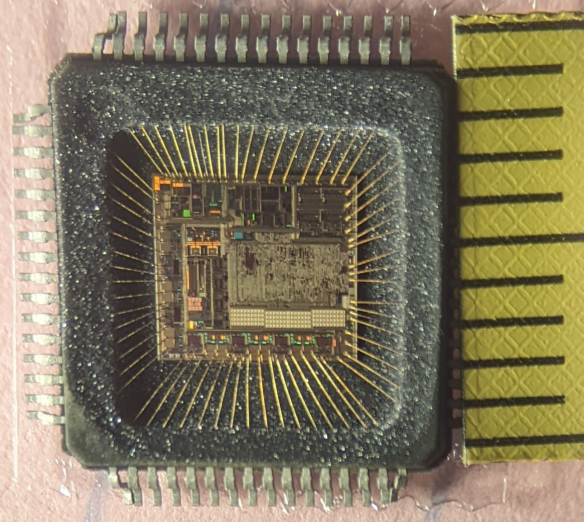
| 
| Die area: 4.90mm x 4.53mm = 22.2mm2 Channel count: 14 AEC-Q100 |
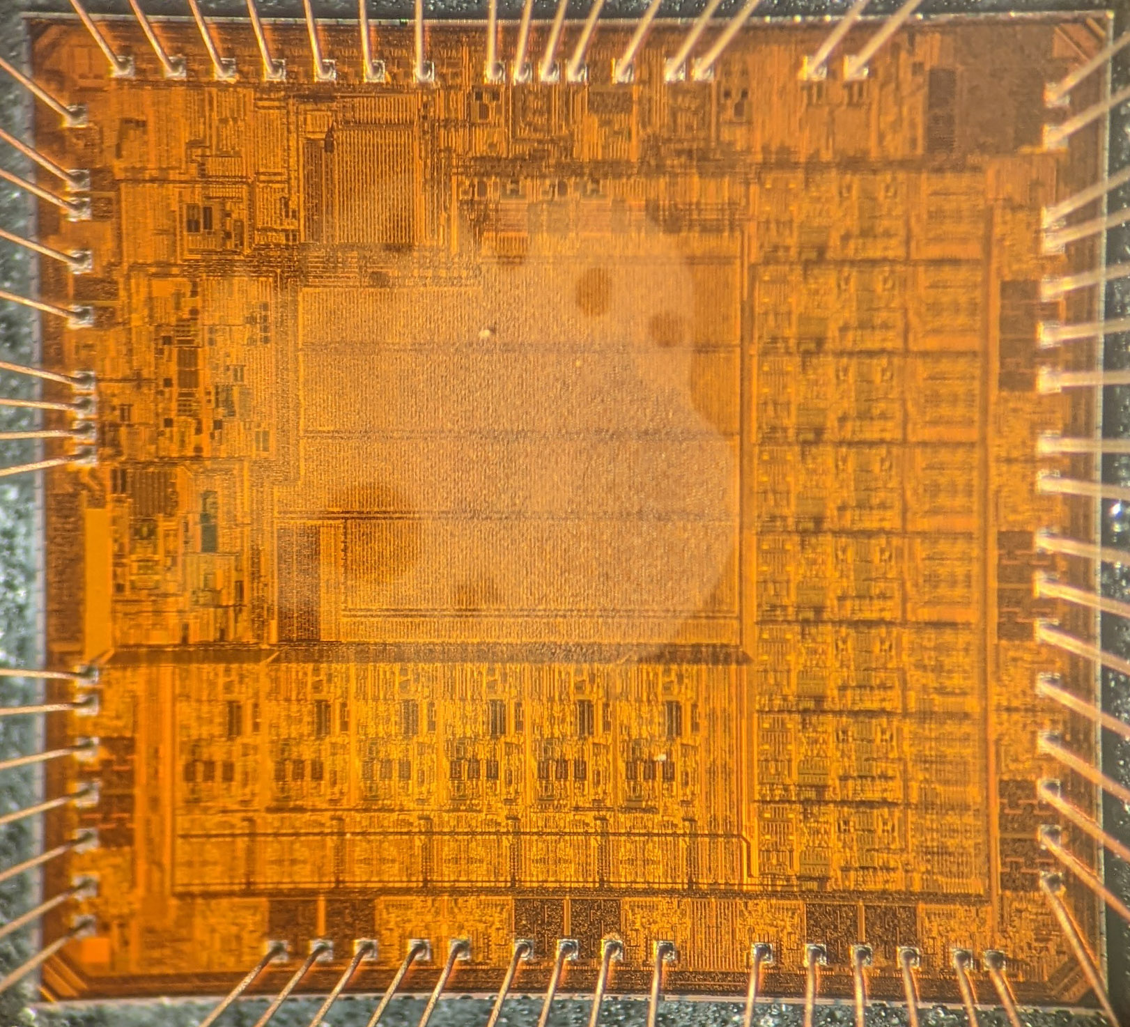
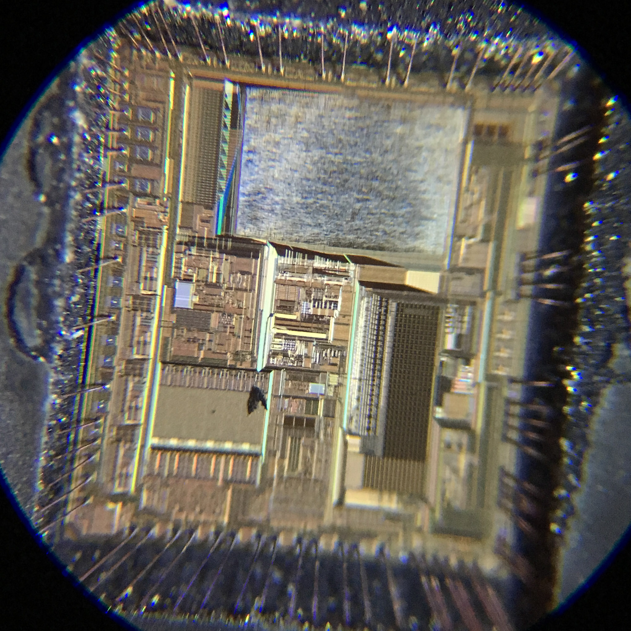
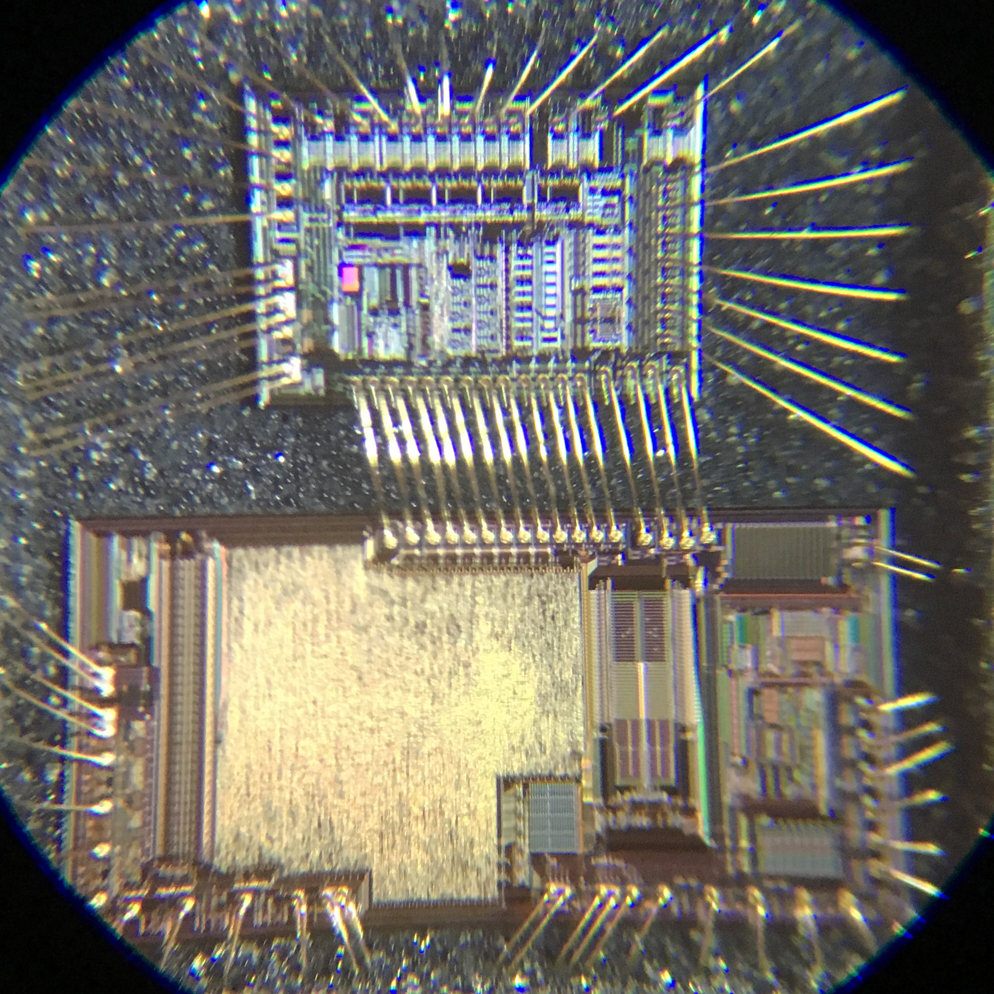
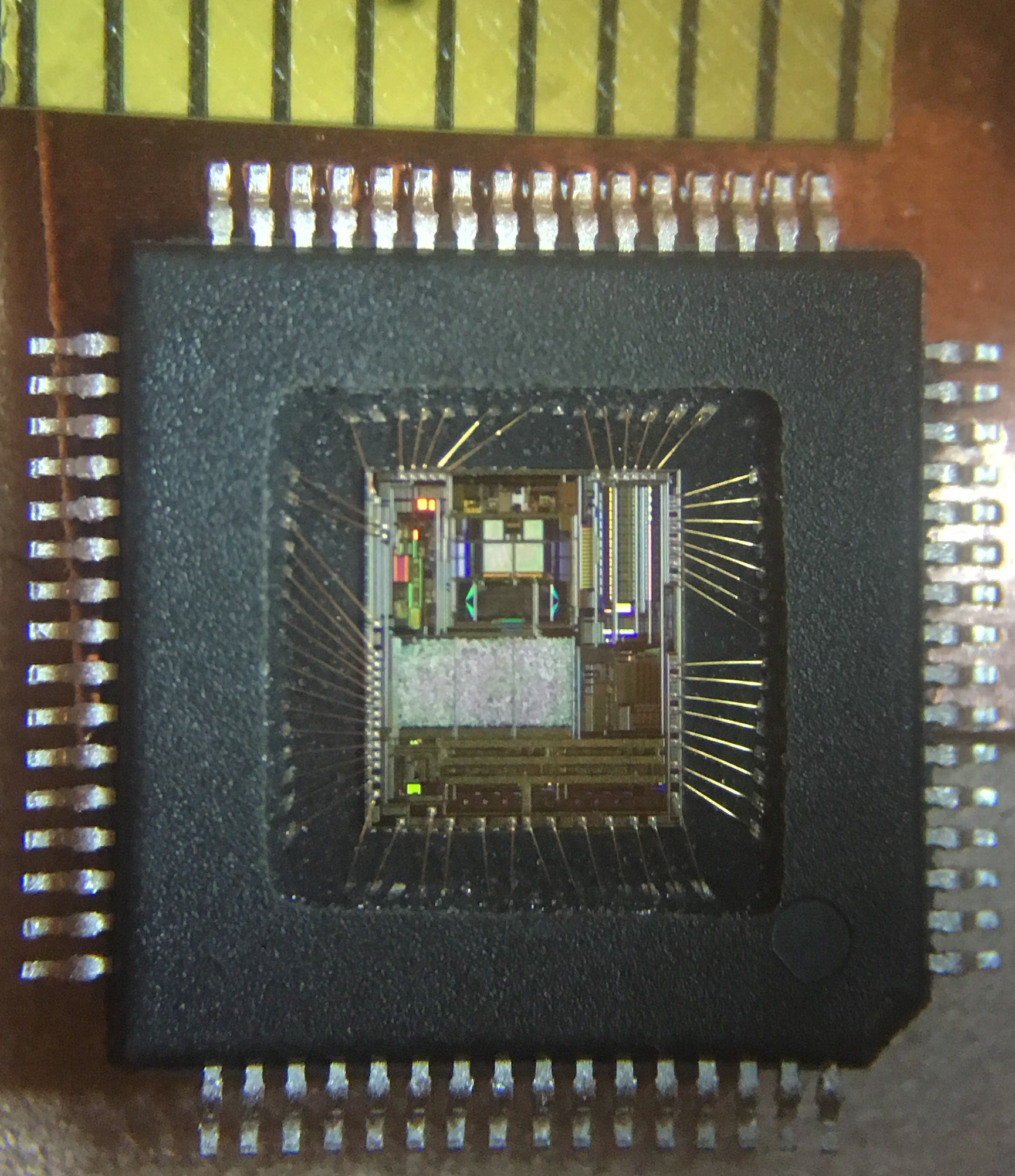
| bq79606 | ||
| 
| Die area: 4.36mm x 4.24mm = 18.5mm2 Channel count: 6 AEC-Q100
|
| LTC6813 | ||
| 
| Die area: 3.61mm x 3.73mm = 13.4mm2 for the larger die Channel count: 18 AEC-Q100 |
| LTC6811 | ||
| 
| Die area: 3.07mm x 2.79mm = 8.6mm2
Channel count: 12 AEC-Q100 |
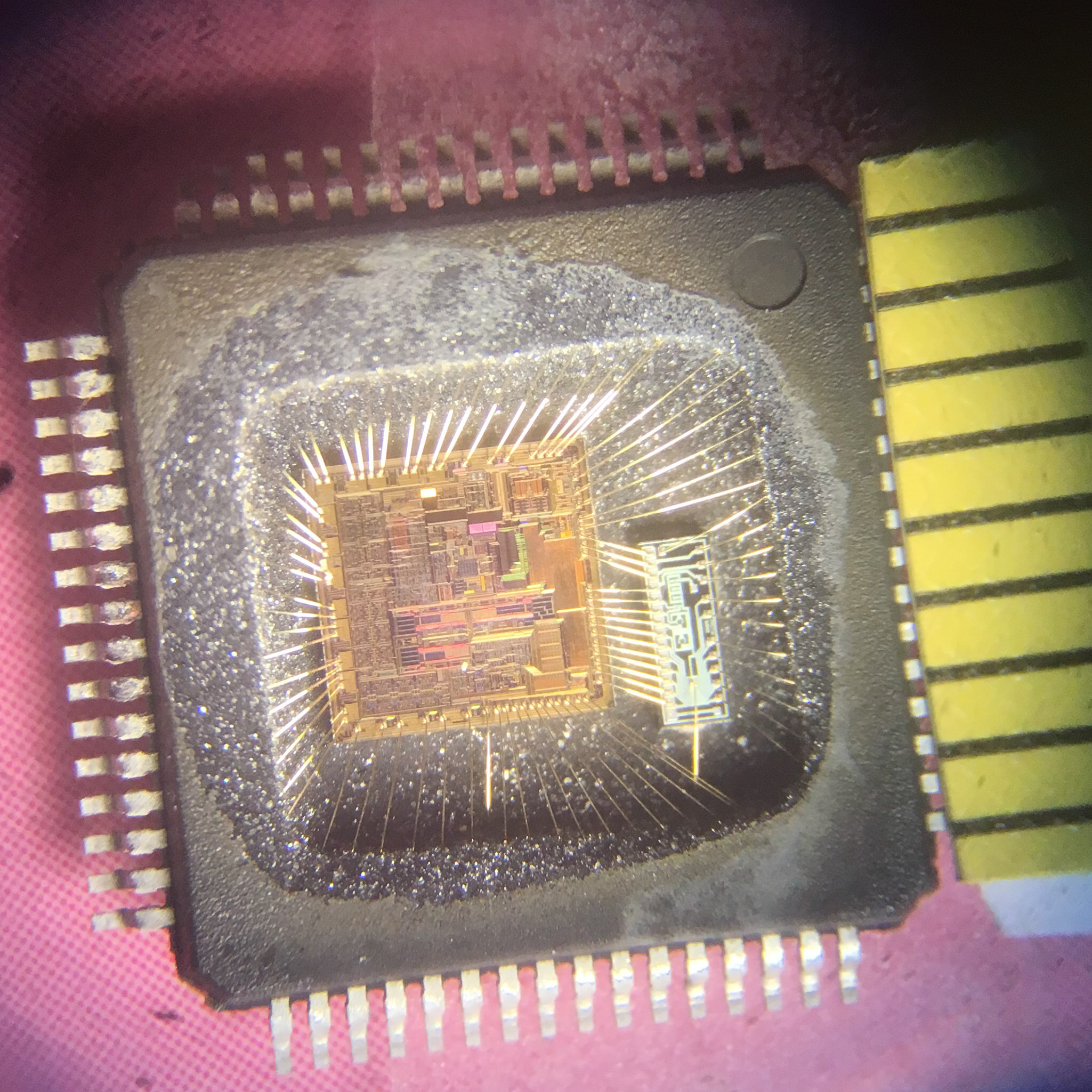
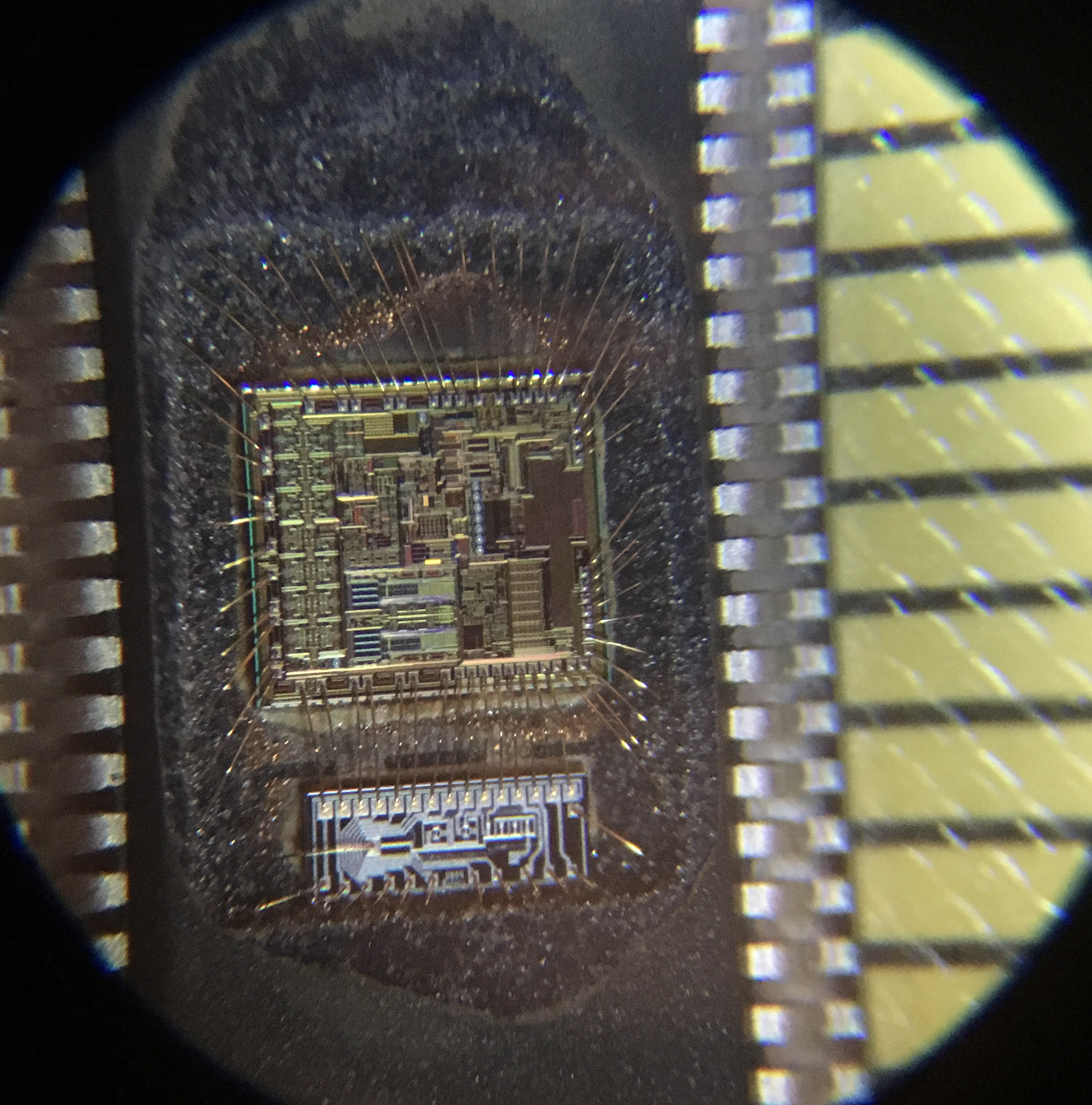
| MAX17823 | ||
| 
| Die area: 4.36mm x 4.15mm = 18.1mm2 Channel count: 12 AEC-Q100 |
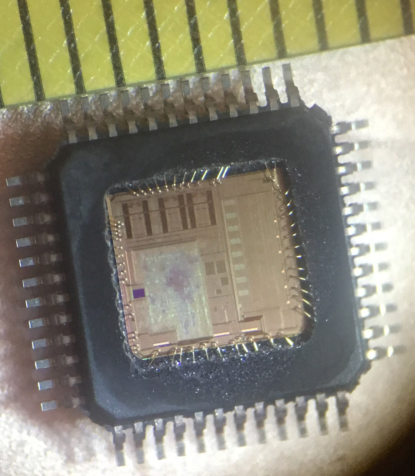
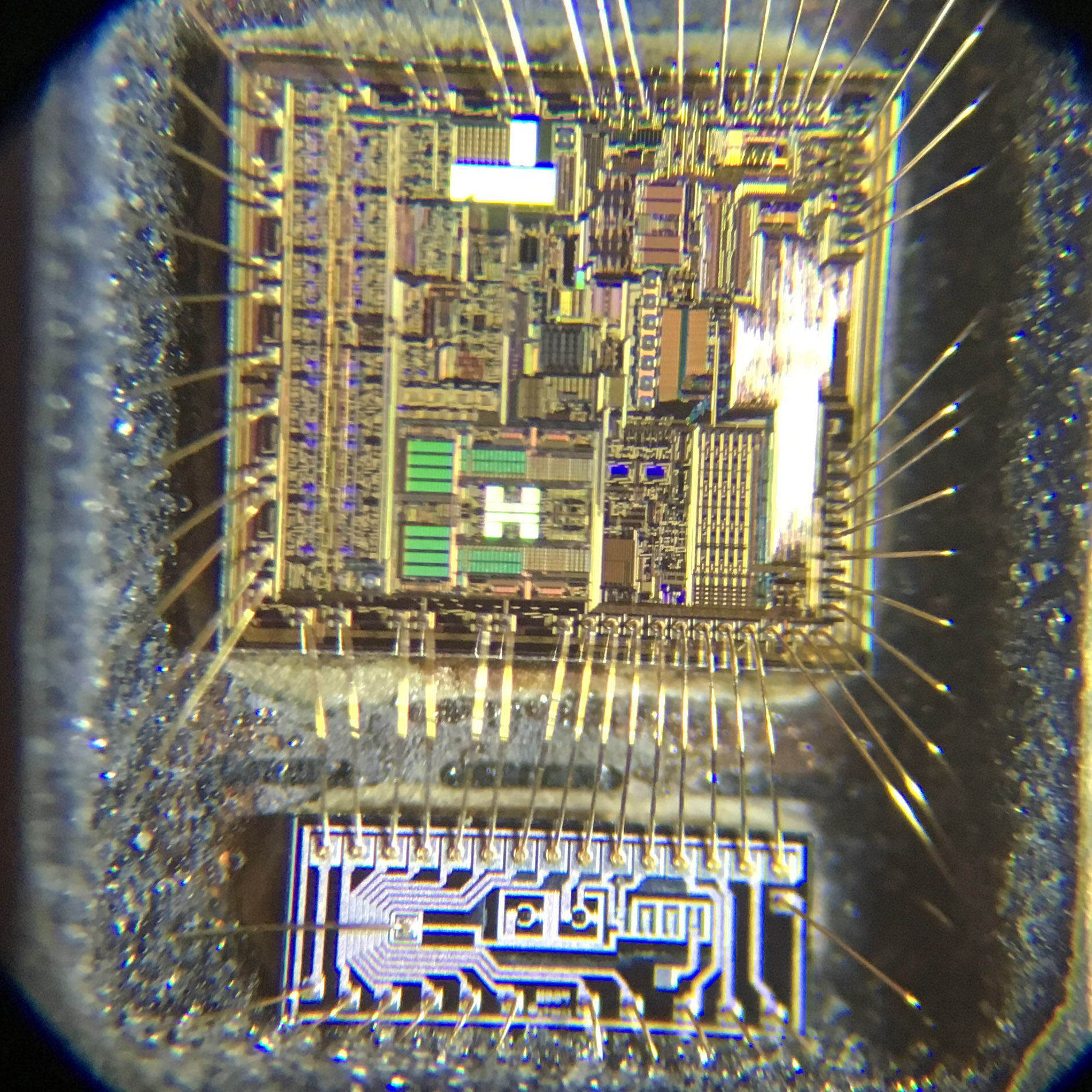
| bq76pl536a | ||
| 
| Die area: 4.31mm x 3.85mm = 16.6mm2 Channel count: 6 Not AEC-Q100 As the Internet will tell you (ex. Jarrod on hackaday.io in comment dated 02/15/2017) this chip was used in the Tesla Model S. |
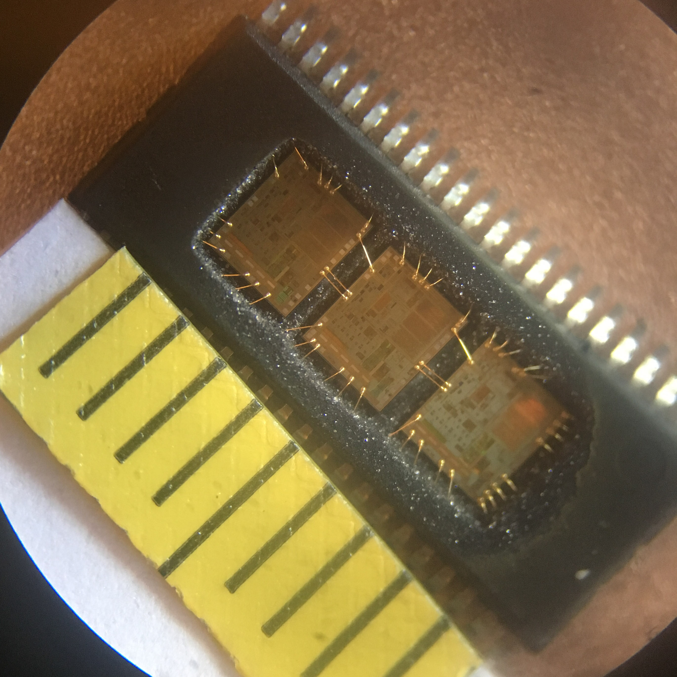
| bq7694003dbt | ||
| 
| Die area: 1.92mm x 2.29mm = 4.4mm2 per die, 13.2mm2 for all three |
| AD7280 | 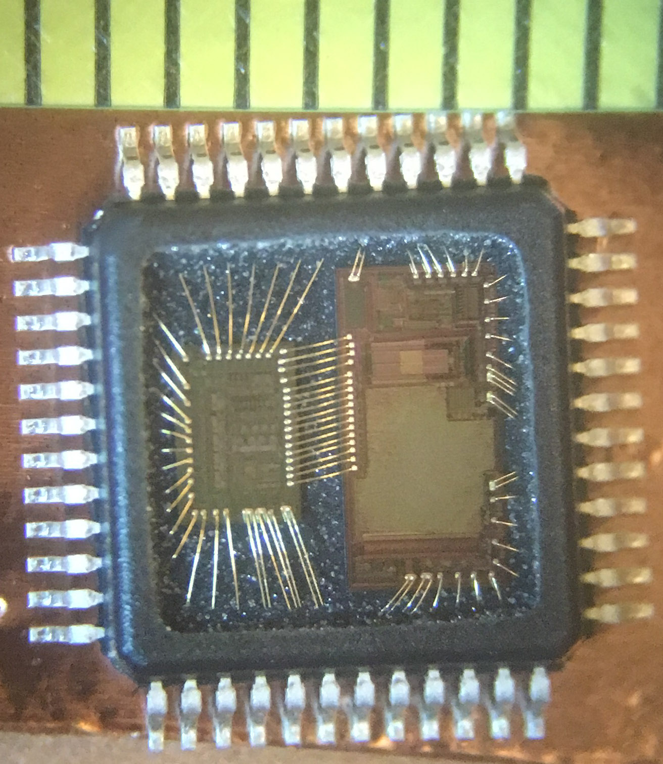
| 
| Die area: 2.32mm x 4.62mm = 10.7mm2
The AD7280 is a fairly old chip, of an older generation. |
| ISL78600 | ||
| 
| Die area: 3.90mm x 4.43mm = 17.2mm2 I got the ISL78600 from some sketchy Chinese web site, if I recall well. |
| LG | ||
| 
| Die area: 4.36mm x 3.80mm = 16.6mm2 |
Back to Ania's Home Page