Visual sensor with resolution enhancement by mechanical vibrations
Koch Lab
Ania Mitros and Oliver Landolt
(In Romanian, translated Apr 2012)
Abstract:
The resolution of both biological and man-made vision systems is limited by the finite spacing between receptors. This limit can be overcome by applying continuous low-amplitude vibrations to the image or taking advantage of existing vibrations in the environment. Some animals rely on this principle for improved visual resolution. We are applying it to a novel CMOS visual sensor to increase resolution and decrease fixed pattern noise.
Biological Inspiration and Technical Motivation:
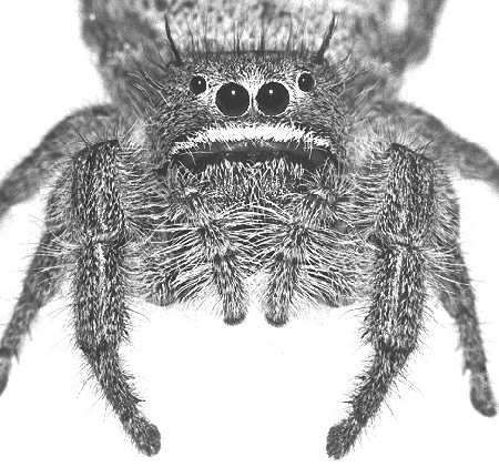 |
Fig. 1 A jumping spider (family Salticidae). These spiders have three pairs of low resolution eyes along the sides of their heads and one large pair of higher resolution eyes on the front. These large eyes contain long but very narrow retinae. In order to see more than just a stripe of the world, the spider actively scans the retinae across the visual field to acquire more information. This principle is analogous to that implemented in our visual sensor. Photo by David Edwin Hill (used by permission) |
Visual sensors found in some living organisms appear to rely on the principle of using mechanical movement of some part of the visual system to increase the amount of information acquired. Jumping spiders are known to acquire visual data by sweeping an essentially linear retina back and forth perpendicularly to its larger dimension, while slowly rotating the retina in its own plane. These spiders are capable of complex visual prey/mate discrimination and route finding tasks using two scanning retinae containing only about 800 photoreceptors each. The human visual system also exhibits minute vibrations of an amplitude close to the smallest intercone separation. If the eyes are immobilized, images fade in a matter of seconds. In addition to preventing such fade-out, it has been postulated that these movements may be used to diminish the resolution limits imposed by intercone spacing.
Man-made vision sensors have not achieved nearly the performance of biological vision systems. Most CCD and CMOS imagers require serial read-out with subsequent computationally- and time-intensive processing. Neuromorphic visual sensors with focal plane processing to parallelize some of the computations are limited in resolution because most of the chip area is consumed by processing electronics instead of photoreceptors. Fixed-pattern noise due to device mismatch in photoreceptors and processing circuitry further limits performance. These effects limit the applicability of existing neuromorphic visual sensors to real-world problems.
We propose to apply a technique to improve the resolution of imagers with focal plane processing. We employ continuous low-amplitude vibrations on the order of pixel spacing along the optical path. Spatial intensity gradients turn into temporal intensity fluctuations which are detected and processed by every pixel independently from the others. This approach enhances resolution by allowing each pixel to gather information in time, and virtually eliminates fixed-pattern noise by permitting the detection of local features without interpixel comparisons. We have designed and implemented an integrated circuit which incorporates this visual sensing principle. It consists of an array of 32 by 32 pixels with local temporal signal processing, and a novel non-arbitrated address-event communication scheme providing timing guarantees on external signals for easy interfacing with off-the-shelf digital components. Furthermore, we have designed and implemented two methods of generating the required mechanical vibrations.
The Concept:
The resolution of visual sensors is limited by the quality of optics, the number of photoreceptors, and the photoreceptor spacing. An increase in the number of photoreceptors directly translates into a proportional increase in the amount of information that the sensor can acquire. Increasing the size of an imaging array is thus the most common approach for improving image resolution. For imagers which perform no on-chip processing, the only cost involved with this approach is an increase in the size of the die and the resulting development and monetary expense to assure quality over the entire area of the die. For vision sensors which incorporate focal plane processing (to parallelize computations and reduce the amount of data to be transmitted off-chip), increasing the number of photoreceptors requires limiting the amount of processing circuitry per pixel.
We propose another not mutually exclusive approach: to allow each pixel to gather information in time. Because an electronic pixel can function on a much faster time scale than the frame rate necessary for many purposes, such as navigation or certain types of visual inspection, each pixel of the imager can reasonably be made to sample several points (or scan a continuous path) in space. The information capacity of such a dynamic visual sensor is greater than that of a static counterpart for scenes that change slowly relative to the sampling or scanning rate. This increase in information can translate into higher resolution. Furthermore, the information from a single pixel can be used to extract information about local image features while avoiding the pitfalls of fixed pattern noise, since neighboring pixels are not compared.
 |
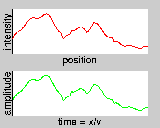 |
| Fig. 2 Lena. Each green circle in the left half of the image represents the path viewed by a single pixel in an array. One path is singled out. | Fig. 3 Conversion of a signal in space to a signal in time. As a pixel scans over part of the image, it senses light intensity changes in space and encodes them as the amplitude of a current signal in time. |
To better understand this principle, consider how we might process the image of Lena in Fig. 2. Each green circle represents the path scanned by a single pixel. A single pixel converts the local spatial signal into a temporal signal, perhaps such as the one shown in Fig. 3. As long as the pixel is able to gather more than a single intensity measurement before the image changes, the information collection capacity of each pixel is increased due to scanning. The scanning frequency must be high enough that a local area can be scanned before the image changes (akin to frame rate), but not so rapid as to blur the features that the pixel is attempting to detect. The amount of blur is inversely proportional to the pixel bandwidth, necessitating careful pixel design to maximize temporal bandwidth.
We have considered the cases of regular scanning, as shown in Fig. 2, as well as irregular scanning patterns. The details are not discussed here. The mechanics for generating both types of vibrations are described below.
Signal Processing:
The continuous waveforms delivered by the photoreceptors carry high-resolution visual information, but this information is not yet encoded in a format suitable for machine vision applications. Additionally, the huge amount of information available in the analog waveforms would be impractical to send off-chip. Local signal processing is performed by each pixel to encode key features in the temporal waveform in a format compatible with off-chip communication.
 |
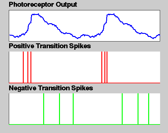 |
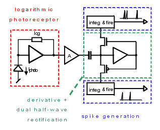
| Fig. 4 Schematic of the internals of a single pixel, described more fully in the text. | Fig. 5 Conversion of the analog photoreceptor output to asynchronous digital form, akin to "spikes" fired by neurons. Each pixel transmits spikes along two channels, one representing positive transitions in light intensity and the other negative transitions. The photoreceptor output shown might be that from scanning twice over the same path, as in the case of periodic circular scanning. |
As shown in Fig. 4, the light intensity is first gathered by a photodiode. This current signal is applied to a logarithmic current-to-voltage converter. When the same visual scene under different illumnations is presented, the output of the photodiode differs only by a scaling factor for the two scenes. The output of the logarithmic circuit differs only in the DC component for the two images, which is ignored by subsequent stages. The visual data thus becomes independent of illumination level. The next processing stage is a differentiator followed by half-wave rectification, wherein both the positive and the negative fractions are retained separately. Each of these is sent on to a non-leaky integrate-and-fire circuit. Thus, one or more spike are produced for every rapid intensity transition such as those corresponding to high-contrast edges. Fainter edges or gradients will result in fewer spikes, perhaps requiring the pixel to scan over the feature several times before unambiguous detection and localization. The cartoon in Fig. 5 illustrates the precise timing and rapid generation of spikes resulting from a sharp transition, and a lower spiking frequency coupled with less precise localization of the spikes for a shallower gradient.
To understand how such a spike train may be processed, consider the case of periodic circular scanning. If the scanning path of the pixel crosses a salient feature such as a high contrast edge, one or more spikes will be reliably generated at a very precise point in time. The information about the existence of such a sharp edge will be immediately available to post-processing circuitry. The precise location of the edge can be determined from the phase in the cycle when the spikes occur. If, on the other hand, a lower contrast edge or gradient is presented, spikes can be histogrammed over several cycles. Because the probability of a spike is directly proportional to the derivative of the intensity signal at any point, given enough scans, the location and magnitude of even the faintest edge can be detected. Similar schemes are possible for irregular scanning patterns, with the modification that a 2-dimensional histogram is required to represent the area scanned by the pixel.
Off-Chip Communication:
The most common technique for transmitting information from an imaging array to other circuitry involves the serial read-out of all pixels and transmission of digital values encoding the level of activity at each pixel. Such a scheme forces the quantization of time into bins of hundreds or, at best, tens of nanoseconds, depending on the maximum possible frame rate. Because our signal encoding scheme relies on precise temporal localization of asynchronous events we chose an alternate scheme, namely address event representation (AER). The underlying premise of AER is that the activity of a pixel can be represented in the frequency and timing of digital spikes (similar to neuronal action potentials in biology). Since the pixels are not clocked, the timing of spikes from different pixels is asynchronous and independent. The activity of the pixel array can then be described by a list of events { (x0, t0), (x1, t1), (x2, t2), ... } describing the locations xi and corresponding times ti when events occurred. Since the events are broadcast off the chip in real-time, ti is not explicitly encoded. This manner of information transmission allows active pixels more frequent access to the bus (and thus more bandwidth) than quiescent ones.
Although versions of this general idea have been implemented by others, we chose to design a novel implementation reflecting design choices most optimally suited to our purpose. A major concern in AER design is the resolution of collisions, or in other words, simultaneously occurring events. Two broad categories of solutions exist:
Unarbitered systems allow all pixels access to a shared output bus. This requires minimal hardware overhead on the chip and minimal transmission delays. However, simultaneous spiking causes one pixel to corrupt the address broadcast by another. Careful choice of the address encoding scheme and use of a non-dense bit code can allow collision detection. Off-chip circuitry must be able to handle no guarantees on the length of time for which data will be displayed; and it must be able to perform this error detection in real time. This is a hefty requirement, given expected data transmission rates on the order of 3 million addresses per second for our system.
Arbitered systems include some on-chip circuitry for collision detection and a graceful method of deciding which of the simultaneously active addresses will be transmitted. Multiple solutions exist: all colliding spikes may be lost; colliding spikes may be pipelined, introducing delay but retaining all data; or an intermediate solution with a limited buffer can be chosen.
To allow our chip to interface with off-the-shelf digital components, we used an arbitered scheme. Since timing is crucial in our system, we designed our AER arbitration hardware to have a short latency at the cost of having only a one spike buffer. Error checking is integrated into the design such that only valid addresses are transmitted off the chip, and a hand-shaking protocol ascertains that all data is cleanly read before a new address is broadcast.
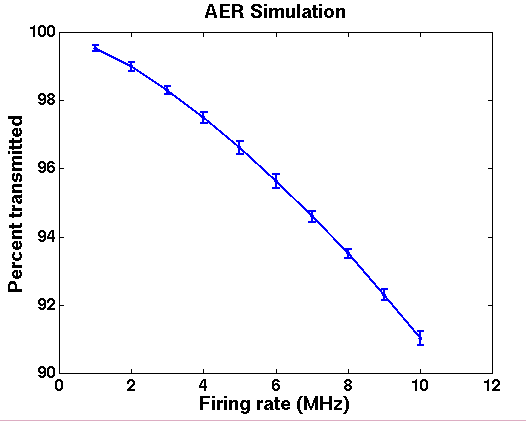 |
Fig. 6. To determine the number of lost spikes due to collisions, we have run simulations. As the number of spikes transmitted by the array increases, the probability of a collision also increases. We have found that acceptable collision rates permit transmission of up to about 7,000,000 addresses per second. For a 32 by 32 pixel array with a scanning frequency of 300Hz, an average firing rate of up to 23 spikes per scanning cycle can be allowed. |
The Chip:
| The chip has been manufactured in a 0.6 micron, double poly, triple metal CMOS process. The chip is designed for a supply voltage of 3V. The pixel array occupies 2.2mm by 2.2mm and the entire chip area is about 10mm2. | 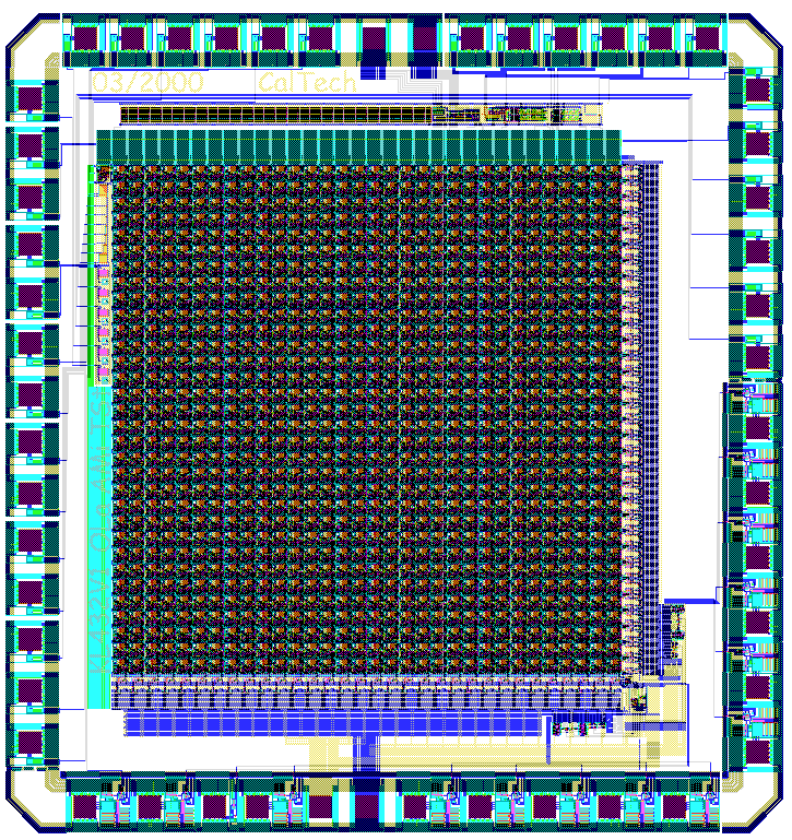 |
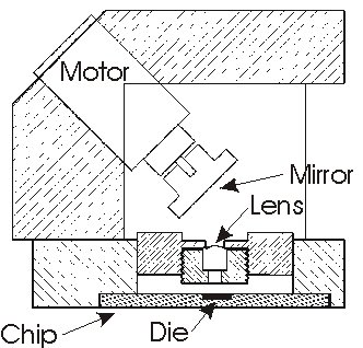
Mechanics for Generating Vibrations:
In order to impose some sort of regular scanning of the image, we can vibrate some element of the optical path: the whole system composed of the chip and the lens, or just the lens, or a mirror positioned in front of the lens, or a prism positioned either in front or behind the lens. We have designed two systems for achieving such vibrations of the image.
 |
 |
| Fig. 7 Left: Schematic of the mechanism for generating periodic circular scanning. Right: photograph of the same. The mirror is mounted on a motor, which is in turn mounted at an approximately 45 degree angle. The surface of the mirror slants at less than 1 degree from the perpendicular to the motor shaft. Thus, as the motor spins, the image reflected by the mirror wobbles in a circular periodic pattern. An encoder on the motor permits knowledge of the angle of the mirror at any time point. The image is focused through a lens onto the chip. | |
 |
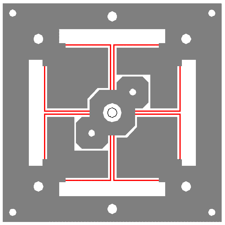 |
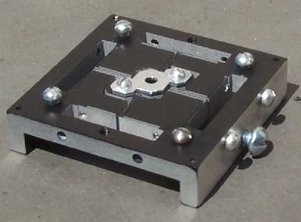 |
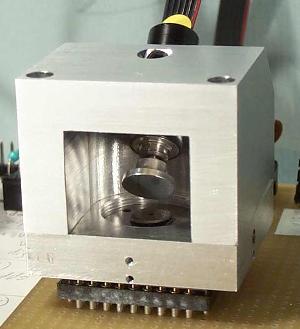
| Fig. 8 The mechanism for generating irregular scanning movements. The lens is suspended in the central circular chamber on four metal springs. The mass of the lens and lens holder as well as the stiffness of the springs determines the target resonant frequency. Vibrations in the environment are amplified near the resonant frequency. These vibrations can be either naturally occurring (resulting from driving over rough terrain, a running motor, etc.) or intentionally induced (for example, with a piezoelectric). Left: Cartoon of the design. Center: Top view of the design (to scale). The thin red lines indicate the springs, which attach the external mass to the central mass. The lens is located in the central circular hole. The remaining holes are for various screws. Right: Photograph of the fabricated mechanism. The lens fits under the central light-colored metal piece. The springs are very thin L-shaped metal strips which cannot be seen easily here. | ||
Sponsors
Engineering Research Centers Program of the National Science Foundation under Award Number EEC-9402726; and U.S. Department of Defense through the Defense Advanced Research Projects Agency (DARPA) and the Office of Naval Research (ONR).
Last updated 28 August 2000 © Anna MitrosBack to Ania's Home Page